
A startup called Black Semiconductor has built an optical chip using graphene—a material just one atom thick—and they’re constructing a factory to mass produce it. This isn’t just another incremental improvement; it represents a potential paradigm shift in computing architecture.
The Copper Bottleneck
Today’s chips move data using electrons traveling through tiny metal wires. This approach has served us well for decades, enabling faster phones and powerful AI processors. But we’re hitting a wall.
As we pack more transistors onto chips, the copper wires connecting them become so thin that resistance increases dramatically. This creates heat and slows everything down. It’s like driving a high-performance sports car on a muddy trail—it works, but it’s far from optimal.
The interconnects between transistors have become one of computing’s biggest bottlenecks. While much attention focuses on transistor density, these tiny wires are quietly limiting our progress.
Enter Light and Graphene
Physics offers an elegant solution: instead of moving electrons, we could move photons—particles of light. Light doesn’t lose energy the way electricity in copper does. It’s faster, runs cooler, and excels at moving data around chips and data centers.
When it comes to controlling light at the nanoscale level, graphene keeps appearing as the material of choice. Why? Because graphene is exceptional at manipulating light on incredibly small scales.
Graphene’s structure is remarkable:
- It’s a single layer of carbon atoms arranged in a perfect honeycomb pattern
- This arrangement makes it stronger than steel yet light and flexible
- Its crystal structure allows electrons and photons to move through with almost no resistance
The numbers tell the story. Graphene’s electrical mobility is around 200,000 square centimeters per volt-second, while silicon’s is just 500. This isn’t a small improvement—it’s a revolutionary difference comparable to upgrading from dial-up internet to fiber optics.
How Graphene-Based Optical Computing Works
To use light for data transmission or computation, we first need to encode digital signals into light. The key device for this is an optical modulator, commonly a Mach-Zehnder interferometer.
This device splits light into two paths, then recombines them. By applying a digital signal to one path, we can shift the phase of the light, altering how it interferes when recombined. This effectively encodes digital bits into light intensity.
While silicon photonics already uses this principle, graphene takes it to another level. Silicon works best in a narrow infrared range, but graphene interacts well with a wide spectrum from visible to infrared and even terahertz frequencies.
What makes graphene truly special is that we can control how much light it absorbs by applying an electrical pulse. This makes it perfect for next-generation optical modulators that switch faster and can be much more compact—easier to scale for mass production.
Beyond Data Movement: Computing with Light
This technology doesn’t just move data faster—it opens the door to computing with light itself. With minor modifications, the same optical modulators can perform multiplication operations.
By applying analog voltages instead of digital pulses, the phase shift changes smoothly, making the output light intensity proportional to the product of input light and applied voltage. This performs analog multiplication—the fundamental operation behind AI workloads.
The beauty of this approach is that light can carry multiple data streams on different wavelengths simultaneously. This enables not just fast computation but massively parallel computation with minimal energy loss.
The Manufacturing Challenge
If graphene is so promising, why isn’t it in every device already? The answer lies in manufacturing challenges.
Making graphene in a lab is one thing; manufacturing it at scale while keeping it flawless is entirely different. When produced in large quantities, defects like grain boundaries and impurities can destroy performance.
Silicon manufacturing took decades to perfect. For graphene, this recipe doesn’t exist yet. Even when it does, graphene must integrate with existing fabrication facilities built around silicon—requiring expensive retooling.
There’s also the transfer problem: graphene is often grown on materials like copper or silicon carbide, but moving it to a chip-ready surface without damage remains challenging.
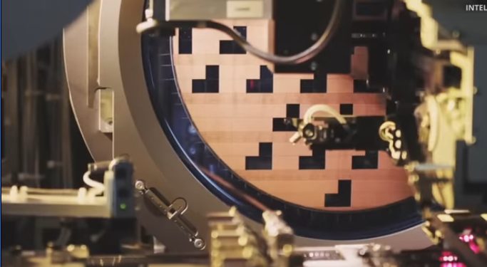
Despite these hurdles, progress is accelerating. Companies like Black Semiconductor are building dedicated graphene fabrication facilities, with production planned to begin in 2026. Others like Destination 2D and Paragraf are developing techniques to move graphene from lab to commercial production.
Even industry giants like TSMC, Intel, and Samsung are exploring graphene integration, starting with hybrid graphene-metal approaches as a strategic transition away from copper.
The question is no longer if graphene will reach the market, but when. As AI computing demands continue to grow, the pressure on interconnects intensifies—creating the perfect opportunity for graphene and photonics to shine.
Frequently Asked Questions
Q: What makes graphene better than silicon for electronics?
Graphene allows electrons to move through it as if they have no mass, with electrical mobility around 400 times higher than silicon (200,000 vs. 500 square centimeters per volt-second). It’s also just one atom thick, stronger than steel yet flexible, and interacts with a wide spectrum of light, making it ideal for optical computing applications.
Q: When will we see graphene-based electronics in consumer devices?
Mass-market consumer devices with graphene components are still years away. Companies like Black Semiconductor are building production facilities with plans to begin manufacturing in 2026, but initial applications will likely be in specialized data center equipment before reaching consumer electronics.
Q: What are the main obstacles to graphene adoption?
The primary challenges are manufacturing at scale without defects, integrating graphene with existing silicon-based fabrication processes, transferring graphene to chip surfaces without damage, and making the production economically viable. These are significant hurdles that require substantial investment and research to overcome.
Q: How does optical computing with graphene compare to quantum computing?
While quantum computing aims to solve specific problems through quantum mechanics principles, graphene-based optical computing offers improvements to conventional computing through faster data movement and analog computation. Optical computing could be commercially viable sooner and addresses immediate bottlenecks in AI and data processing, while quantum computing represents a more fundamental departure from classical computing with a longer timeline to practical applications.
Q: Which companies are leading in graphene technology development?
Several companies are pioneering graphene technology: Black Semiconductor is building graphene-based photonic chips and a manufacturing facility in Germany; Destination 2D (a UC Santa Barbara spin-off) is developing graphene interconnects and fabrication techniques; Paragraf has developed methods for growing high-quality graphene at scale; and major semiconductor companies like TSMC, Intel, and Samsung are exploring graphene integration into their processes.