In Arizona’s desert, two visions for chipmaking face off. One is patient and careful. The other is high-wire daring. I believe the daring one—Intel’s—could reset power in advanced manufacturing. But it will only matter if Intel turns a brief lead into dependable output and trusted partnerships.
A Bold Factory With Hard Limits
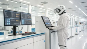
Intel’s Fab 52 is a feat of scale and control. The clean room spans about 700,000 square feet. Air gets cycled hundreds of times per hour through ULPA filters, making it far cleaner than a hospital.
The water challenge alone reads like a civic project. One wafer can use around 22,000 gallons of ultra pure water. At full tilt, the site draws about 9 million gallons per day, then recovers roughly 80% through a dedicated recycling plant. That is the price of precision in a dust-prone desert.
And then there are the tools. Intel was first to install High-NA EUV for production. As the engineer explains:
“Each one cost about $380 million, weighs 180 tons, and must be shipped in multiple cargo flights.”
Being first with High-NA EUV gives a real hardware edge. But tools do not win alone. Yield does.
The Real Breakthrough: Power From Below
Intel’s 18A node is not just smaller; it is different. The company changed the transistor and the power network in one stroke—defying the industry’s “one big change per node” rule.
- RibbonFET replaces FinFET, wrapping the channel on all sides for better control.
- PowerVia brings power from the backside of the wafer, freeing frontside routing.
Why this matters: IR drop and routing congestion were choking progress. By moving power under the transistors, Intel shortens the path, cuts loss, and opens space for signals. As the engineer puts it:
“For the first time in semiconductor history, power no longer comes from the top of the chip. It comes from the back side of the wafer.”
Intel claims around 30% lower power losses and higher logic density. If those gains hold at scale, the blueprint for future chips is set.
Speed Now, Pain Later?
Skipping the safer “20A” step saved time but invited chaos. Early 18A yields were under 10%. Alignment, deposition, and new failure modes collided. Months of grind lifted numbers enough to ship the first Panther Lake processors in early 2026. The lesson is blunt: speed carries a bill, and yield is the invoice.
Meanwhile, TSMC stayed conservative with N2, phasing changes to protect yield and reliability. Intel grabbed the lead; TSMC grabbed certainty. Samsung is pressing similar ideas. This window will not stay open for long.
Why Trust, Not Tools, Is Intel’s Hurdle
Intel wants outside customers for its foundry. But it also sells CPUs that compete with those customers. That tension—well known as the IDM dilemma—never troubled TSMC. Companies like AMD trust the neutral path.
NVIDIA’s $5 billion commitment helps, but it is a hedge, focused on test runs and chiplets. TSMC capacity is stretched by AI demand. NVIDIA needs a backup. Washington needs a domestic option. Intel needs credibility.
The question is no longer “Can Intel build it?” It is “Will customers bet their roadmaps on it?”
What I Think Should Happen Next
To turn promise into staying power, Intel must show consistency, not just headlines. That means repeatable yields, on-time ramps, and a customer model that eases conflict.
- Publish steady yield and defect trends that matter to designers.
- Offer strict firewalls and governance to separate foundry work from product groups.
- Lock in long-term capacity deals tied to transparent milestones.
- Expand chiplet and packaging services where neutral integration wins trust.
- Secure steady High-NA EUV throughput to protect density and cost gains.
The world needs a second top-tier manufacturer at scale. A resilient supply chain depends on it.
I want Intel’s bet to pay off—not for nostalgia, but for resilience. The Arizona build shows grit. The 18A design shows nerve. Now it is time to turn nerve into habit. Hold Intel to yield, delivery, and trust. Ask your vendors where they will build. Push leaders to back domestic capacity with real orders, not press releases.
If Intel converts this fragile lead into reliable output, everyone wins—engineers, customers, and national resilience alike.
Frequently Asked Questions
Q: What makes Intel’s 18A different from earlier nodes?
It combines two big shifts at once: RibbonFET transistors and PowerVia backside power delivery. Together, they aim to cut losses and open routing space for denser logic.
Q: Why is backside power delivery such a big deal?
Feeding power from the wafer’s back shortens the path to transistors, reducing voltage drop and noise while freeing the frontside for signal wires. It attacks two core limits at once.
Q: Didn’t TSMC and Samsung plan similar features?
Yes. Both are moving to gate-all-around transistors and backside power on upcoming nodes. Intel’s edge is timing; the challenge is holding it with yield and volume.
Q: Are High-NA EUV tools the main advantage?
They help by printing smaller features and raising density. But tools alone do not win. Yield, cycle time, and consistent delivery decide who leads.
Q: What should customers demand from Intel Foundry?
Clear yield data, solid timelines, strict separation from Intel’s product groups, and long-term capacity commitments. Reliability and trust must match the technology story.