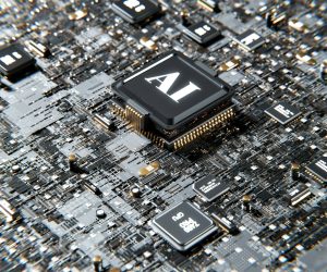
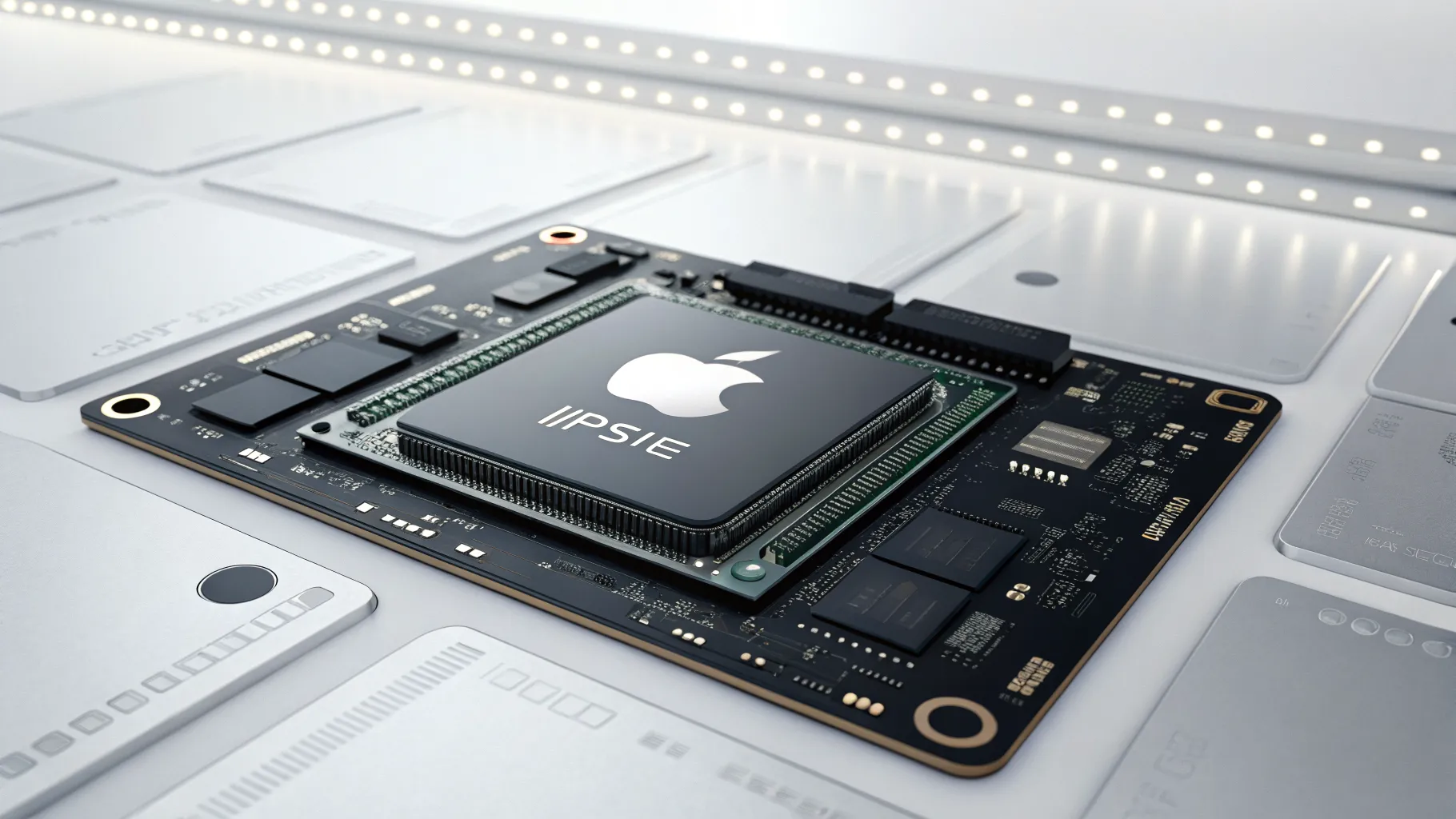
Apple introduced a new chip design that aims to push performance while keeping power use in check. The company said its Fusion Architecture combines two silicon dies into one system. The move signals a fresh step in how Apple plans to scale its processors across devices.
The announcement positions Apple to boost compute capacity without relying only on ever-smaller transistors. It arrives as chipmakers face supply limits, rising costs, and heat concerns. The company framed the approach as a way to deliver higher performance within familiar power and size limits.
What Apple Announced
“The chips are engineered around Apple’s new Fusion Architecture, an advanced design that merges two dies into a single, high-performance system on a chip (SoC).”
Apple described the design as a single package with two dies working together. That package behaves like one SoC to the system. The company suggested gains in compute density and bandwidth. It also suggested better use of limited high-end manufacturing capacity.
Why It Matters
For years, Apple has built its processors as monolithic SoCs. That model helped deliver strong performance per watt in phones and computers. But transistor scaling has slowed. Yields for very large dies can be challenging and costly.
By splitting a design into two smaller dies, Apple can reduce waste when defects occur. Smaller dies often yield better, which can stabilize supply. Packaging advances now make it possible to link dies with fast interconnects inside a single module.
Technical Approach and Trade-Offs
Dual-die designs promise more cores, more cache, and wider memory paths. The key is keeping latency low and bandwidth high between the two dies. Packaging must manage heat and power delivery so performance remains stable.
There are trade-offs. Inter-die links add complexity. Software schedulers must place tasks to avoid bottlenecks. Manufacturing needs tight control to align the dies and maintain signal integrity under load.
- Potential gains: higher performance, better yields, flexible scaling.
- Challenges: latency across dies, thermal hotspots, validation across varied workloads.
Industry Context
Multi-die strategies are gaining traction across the sector. Several chip companies now link smaller chiplets to build larger processors. Advanced packaging, including 2.5D and 3D methods, has matured. This supports short links with high bandwidth and lower power per bit.
These methods address cost and physics limits that slow traditional scaling. They also help companies mix process nodes. A vendor can pair a high-end compute die with a lower-cost I/O die. That can shorten development cycles and broaden product ranges.
What It Could Mean for Apple’s Lineup
Apple did not specify products or dates. Still, the approach suits devices that need high performance within tight thermal envelopes. Laptops and desktops could benefit from more CPU and GPU units. Pro tablets might gain from wider memory bandwidth for media tasks.
If the packaging is efficient, servers and workstations could also see advantages. The key will be sustained performance under long workloads. Battery-powered devices will depend on low idle power and quick ramp-up without thermal spikes.
Developer and User Impact
For developers, thread scheduling and memory locality matter more when resources span multiple dies. Apple’s tools will need to expose performance counters and guidance. Clear APIs can help apps place tasks and manage data paths.
End users may see gains in rendering, video editing, and machine learning tasks. Performance per watt improvements could lengthen battery life at similar speeds. Or they could enable higher speeds at the same battery life.
What to Watch Next
Key indicators will include sustained performance, thermals under load, and software optimization. Supply stability will show whether yields improve as planned. Pricing will hint at packaging costs and volumes.
Competitors will respond with their own packaging advances. The contest now rests on link bandwidth, cache design, and memory systems as much as on core counts. The company’s move suggests that packaging is now as strategic as process nodes.
Apple’s Fusion Architecture marks a clear bet on multi-die design. If the firm delivers low-latency links and efficient thermals, users could see meaningful real-world gains. The next product cycle will reveal how well this design scales, how software adapts, and where the biggest wins appear first.
Rashan is a seasoned technology journalist and visionary leader serving as the Editor-in-Chief of DevX.com, a leading online publication focused on software development, programming languages, and emerging technologies. With his deep expertise in the tech industry and her passion for empowering developers, Rashan has transformed DevX.com into a vibrant hub of knowledge and innovation. Reach out to Rashan at [email protected]