The Growing Gap Between AI and Hardware
Here’s what most analysts miss: while AI capabilities double roughly every seven months (about 3.4× yearly improvement), the underlying hardware only improves by about 1.4× annually. This growing gap creates both challenges and opportunities.
Computer chip advancement happens at multiple levels:
- Device level (the transistor itself)
- Architecture level (how transistors are arranged)
- System level (software and cooling solutions)
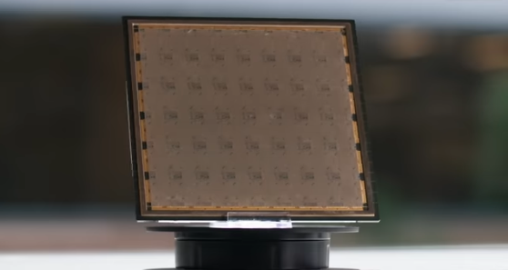
While TSMC manufactures chips at scale, innovation often begins at research institutions like IMEC, which recently released a roadmap outlining semiconductor technology development for the next two decades. Having spent a decade in chip design myself, I find this roadmap fascinating—it shows how we’ll scale from today’s 2nm process down to an astonishing 0.2nm by 2037.
The Evolution of Transistors
The transistor’s journey has been remarkable. We began with simple planar transistors—flat 2D structures on silicon. As we kept shrinking them, we hit physical limits that required completely new approaches.
This led to FinFET technology, where the channel (where current flows) was raised vertically like a shark fin. This gave engineers better control over the current and allowed more transistors to fit in the same space. Most modern chips, including those from AMD and Apple, still use this technology.
But now we’re hitting FinFET’s limits, prompting another revolutionary shift. The newest design, called gate-all-around or nanosheet, essentially lays the fin down and stacks several of them like floors in a building. This gives access to all four sides of the channel, allowing better control at even smaller scales.
This technology is arriving soon—TSMC is bringing it to AMD and Apple chips by the end of this year.
Backside Power Delivery: The Game Changer
Perhaps the most exciting aspect of this new technology isn’t just the transistor shape but how power is delivered. Until now, all wires for power and signaling have been crammed on top of the chip—imagine bringing all plumbing and electricity through your ceiling.
Backside power delivery flips this approach, bringing power connections to the bottom of the chip. This frees up significant space on top for the actual computing work. TSMC and Intel are racing to implement this architecture, which will soon power everything from smartphones to advanced AI systems.
Beyond Silicon: The Future of Materials
According to IMEC’s roadmap, even gate-all-around technology will eventually hit scaling limits around 1nm (or 10 Ångströms). At this point, we’ll need to reinvent the transistor again.
The next major architecture will likely be CFET (complementary field-effect transistor), which stacks gate-all-around devices vertically—like building skyscrapers instead of sprawling outward. This approach could take us to single-Ångström dimensions.
But the most transformative changes will come from new materials beyond silicon. Two-dimensional materials like molybdenum disulfide and tungsten disulfide, just one atom thick, show tremendous promise. Carbon nanotubes (essentially rolled-up graphene) are another candidate, offering high speed and better power efficiency.
These new materials could reduce power consumption dramatically, but manufacturing them at scale presents enormous challenges.
The Memory Wall Problem
While computing power advances rapidly, memory is becoming the biggest bottleneck. SRAM (used for cache) doesn’t scale well with new architectures, consuming more chip area with each generation. DRAM (working memory) scales slowly, and we’re now stacking it in 3D layers.
The CFET architecture finally offers hope for better memory density, but the fundamental issue remains: as compute becomes more powerful through clever designs and algorithms, memory remains relatively slow and power-hungry—especially for AI applications.
What This Means For The Industry And You
As chip manufacturing grows more complex, it also becomes more expensive. While transistor costs may stay flat thanks to better density, the total cost of making a wafer is skyrocketing due to manufacturing complexity.
We need healthy competition between TSMC, Samsung, and Intel to drive progress. Without it, innovation slows and prices rise. For consumers, this likely means more expensive devices and AI services.
For investors, however, this complexity creates opportunity. The semiconductor space remains one of the highest-growth areas in technology, with companies like TSMC, ASML, and Applied Materials positioned at critical points in the supply chain.
The next 15 years will transform computing in ways we can barely imagine today. Those who understand what’s happening at the transistor level will be best positioned to benefit from this revolution—whether as users, creators, or investors.
Frequently Asked Questions
Q: What is Moore’s Law and is it still relevant?
Moore’s Law refers to the observation that the number of transistors on a microchip doubles approximately every two years. Despite being declared “dead” numerous times, it remains relevant as innovations in transistor design, materials, and manufacturing techniques continue to drive semiconductor advancement, albeit through different approaches than simple scaling.
Q: Why are companies like Apple and Google making their own chips?
Tech giants are designing custom silicon because controlling chip architecture gives them significant competitive advantages. Custom chips allow these companies to optimize specifically for their software needs, improve energy efficiency, reduce costs at scale, and create unique features that differentiate their products from competitors.
Q: What is the significance of backside power delivery in chip design?
Backside power delivery represents a fundamental shift in chip architecture by moving power connections to the bottom of the chip instead of the top. This innovation frees up substantial space for signal routing and logic components on the top side, enabling more efficient designs, better performance, and continued scaling of transistor density.
Q: How will 2D materials change computing?
Two-dimensional materials like molybdenum disulfide, just one atom thick, could enable transistors that operate at lower voltages with better power efficiency. This could dramatically reduce energy consumption in computing devices while allowing continued miniaturization. However, manufacturing challenges must be overcome before these materials can be used in mass production.
Q: What is the “memory wall” problem in computing?
The memory wall refers to the growing gap between processing speeds and memory access times. As computing power increases rapidly through architectural innovations and algorithms, memory technology advances more slowly. This creates a bottleneck where processors spend significant time waiting for data from memory, limiting overall system performance, especially for data-intensive applications like AI.